


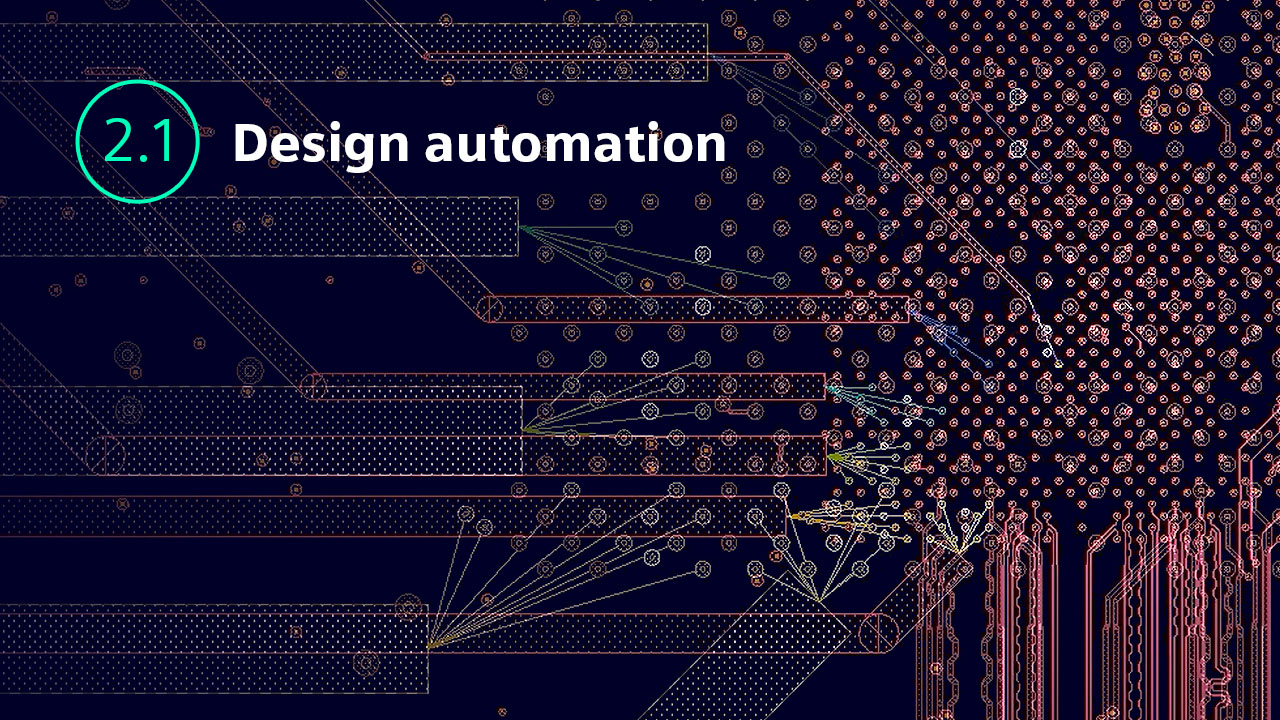
When we think about the PCB design best practices that fall into the engineering productivity and efficiency pillar, we need to start off with design automation.
What is design automation?
When it comes to PCB design software, simply put, design automation is the automation of certain tasks throughout your PCB design process. There are many functions or processes within PCB design that can be automated including:
- Placement: 3D component planning and placement provides correct-by-construction placement while considering electro-mechanical constraints.
- Clusters: Also referred to as Groupings or Unions, Clusters is when specific components within a respective circuit or set of circuits are assigned to a group consisting of many components. Once a group of components are assigned to a cluster, that cluster can be treated as if they are an individual component during placement. These clusters are initially created and defined within the Constraint Editor (CES). Then, when an electrical engineer is selecting components during circuit creation of the schematic, he/she can assign each component to a specific cluster, respectively. Then that specific cluster can be given a unique name that is relevant to the circuitry at hand for a better circuitry identification during the PCB Design process.
- Routing: powerful automated routing technology enables extraordinary efficiency during PCB layout. Unravel complicated net paths and pin escapes to minimize net lengths and quickly and easily identify the best routing strategies. Designers can manually (interactively) route traces or use the automation in auto-routing in a controlled manner, or they can utilize a combination of the two routing processes to achieve their specific routing requirements for overall success.
- Sketch routing: sketch routing provides a set of highly integrated automated routing functionalities featuring intuitive user control, high quality, and exceptional performance.
- Manufacturing output: Whether the outputs contain one specific set of data or several files such as ODB++, IPC-2581, Gerber data, an IPC-356 Netlist, GENCAD data, ICT files, etc., the generation of these file can be automated to be consistent from design to design and or tailored to your internal company standards and or your PCB fabricator and assembly manufacturer.
WhatЁЏs not working?
Legacy methodologies canЁЏt meet todayЁЏs design complexities when it comes to automation regarding optimization and efficiency. ItЁЏs harder to achieve success when doing everything manually, especially with the increased complexities of todayЁЏs products.
What are the roadblocks?
The typical roadblocks that youЁЏll see when moving toward design automation is that PCB designers may be unfamiliar with the automated functions available within their PCB design tool. Using automation can sometimes evoke a feeling of having less control of the design. Current ecosystems could also play a part in preventing the use of automation. One of the biggest roadblocks of the evolution from legacy methodologies is internal company cultures. Having full buy-in and openness to change in evolution is key in achieving success with the best potential for automation optimization and efficiency.
Best practices: design automation
Best practices include assigning parts to groups or clusters and routing using automation (a combination of interactive, sketch, and automated routing strategies). Also generating manufacturing outputs by utilizing built in automation functionality. The value youЁЏre going to get from this is shortened design cycle times, increased layout optimization and efficiency, and the ability to do ЁАwhat ifЁБ scenario reviews, which makes a more optimized and efficient design process. YouЁЏll be able to implement changes more efficiently. YouЁЏll also be able to remove or prevent the potential for errors. And lastly, youЁЏll be able to have consistent manufacturing outputs each time they are generated.
How it works: design automation ЈC placement
When placing components in a layout, one way to speed up the process, besides the utilization of reuse circuitry (reuse blocks or reuse modules), is by using component groups. While reuse blocks assist in adding pre-placed and pre-routed circuits, component groups help keep parts together that may not be part of a reuse block within the library, that should be placed near or within a specific proximity to each other on the board.
Component groups still show the user netline connectivity between themselves and other components, which can help in determining the best placement or location for groups of components. They also are sized based on the size of the components within them, to help determine the board real estate that each group may take up or occupy.
How it works: design automation ЈC routing
When it comes to routing, automation is the key to increasing productivity (optimization and efficiency). While Xpedition has a powerful autorouter, many times it makes sense to use a more manual interactive approach which allows more hands-on control of each, and every signal trace being routed. A what-if approach utilizing the autorouter is a great option to take advantage for routing automation, which increases the potential for routing optimization and efficiency. Lastly, a combination of both autoroute and interactive routing will provide the best and highest potential in achieving success, in regard to routing optimization and efficiency.
Using sketch planner, allows users to start to plan where routes will go, and can even be used before all the components are placed. A good example of this would be when the designer is using sketch planner to create blind sketch plans for single pin routes going to a yet-to-be-placed connector. With the plans created, the pins can be broken out, and routes started. Once the connector is added to the board, using sketch route makes quick work the remainder of the connection.
How it works: design automation ЈC manufacturing output
When the PCB design is 100% completed (all components placed and signals routed), has passed all signal analysis/verification to include manufacturing and producibility analysis/verification, and has passed final reviews, the time comes to generate all the required outputs for board fabrication and board assembly manufacturing. As stated earlier in this blog, generating all the required manufacturing outputs is another area where automation can be taken advantage of to save time and remove redundant steps.
Whether the outputs contain one specific set of data or several files such as ODB++, IPC-2581, Gerber data, an IPC-356 Netlist, GENCAD data, ICT files, etc., the generation of these file can be automated to be consistent from design to design and or tailored to your internal company standards and or your PCB fabricator and assembly manufacturer. The legacy methodology of manually doing each step or task individually to generate each required output file is time consuming, potentially inconsistent each time in generating output files, and prone to potential output files being missed or not generated during the output generation stage of the PCB design process for all the required output files, even if an external checklist is manually being used. Content correctness, quality and consistency is key in setting up your board fabricator and board manufacture for success in producing your required printed circuit assembly.
Visit our website or watch this video to learn more about design automation.